


About us
Beautiful x-ray applications for advanced x-ray scattering and imaging
At PoliMiX we make an innovative use of X rays in fundamental science and industrial applications. Based at the Physics Department of POLIMI – Politecnico di Milano, we collaborate with major synchrotrons and free electron laser x-ray facilities in Europe and with Italian companies producing x-ray instrumentation and systems.
In the past 20 years we have been leading the development of RIXS, resonant inelastic x-ray scattering, an energy-loss spectroscopy used to measure the energy of charge, orbital, spin and lattice excitations in quantum materials.

Latest news
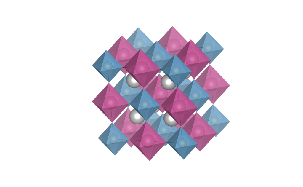
The Hidden Magnetism of Osmium Oxide UnveiledThe study of spin-orbit-coupled Mott insulators […]
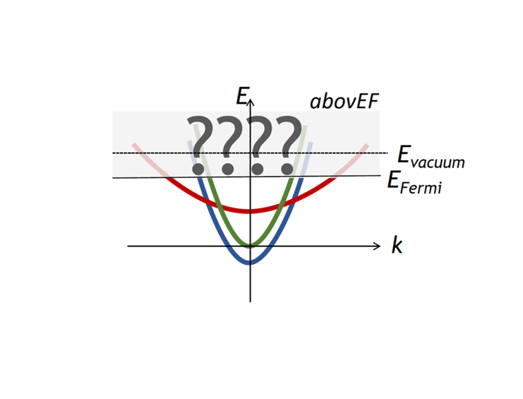
abovEF: A New Frontier in Electronic States Exploration We are excited to […]
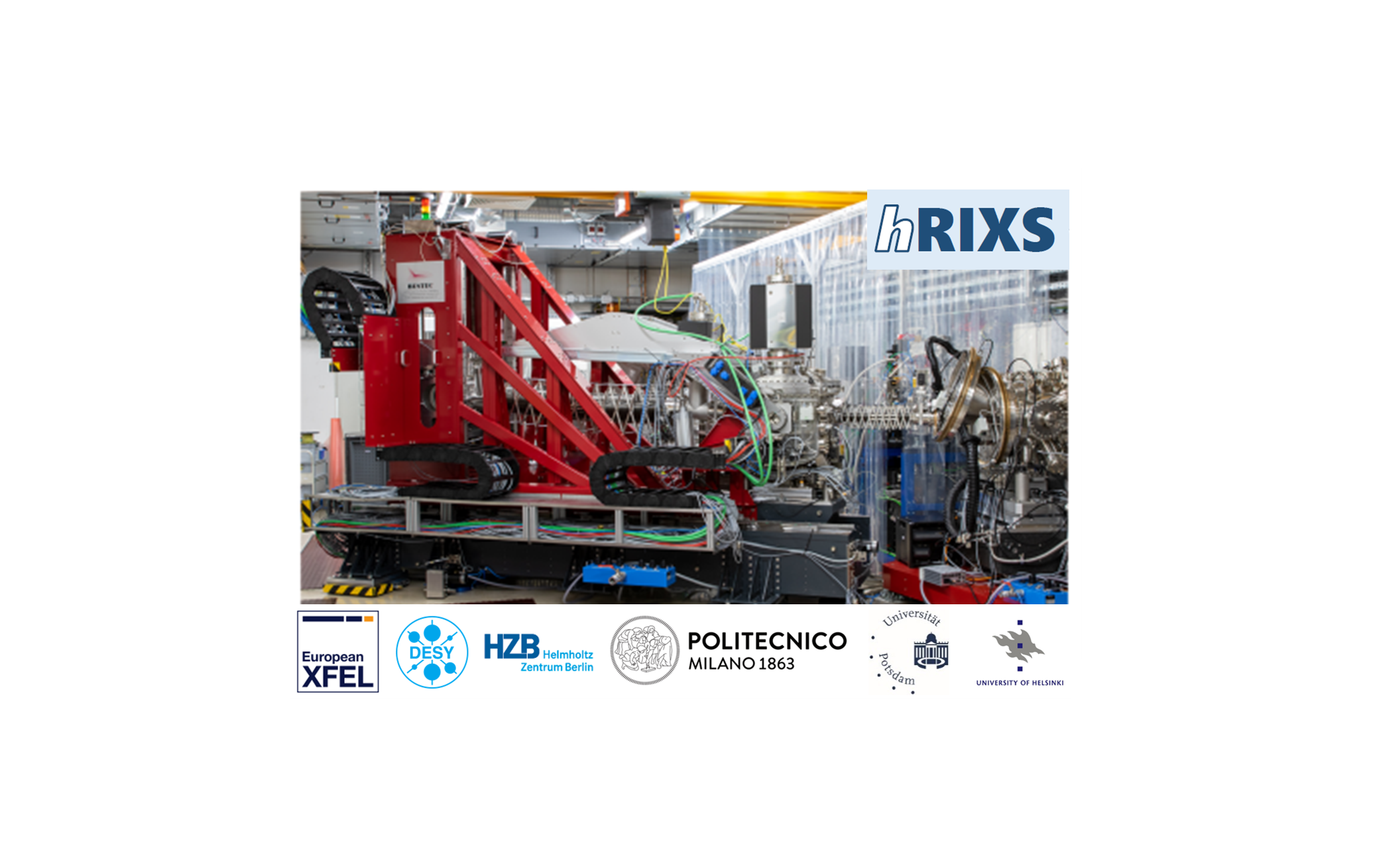
The Heisenberg-RIXS instrument at the European XFEL FELs (Free Electron Lasers) represent […]